Technology Specifications
FORMing
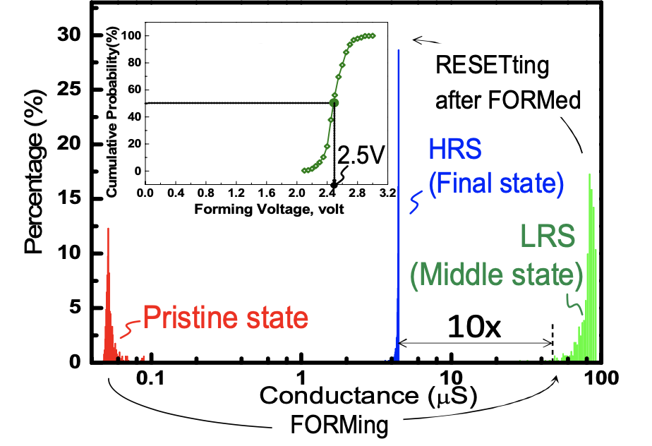
The figure below shows forming data on a 1Mbit RRAM array. At fresh (e.g., unformed) the starting conductance of the RRAM ranges below 0.1 uS (e.g., resistance above 10MOhms). To form the cells, voltages from 2.2 to 3.1V are required (average 2.5V), with very high yields (above 99%) achieved with a max forming voltage of 3.1V. After FORM, the RRAMs end up in an ultra-low LRS of 30-120uS. Resetting the cells after forming results in an HRS. The forming pulse widths are 1,000ns (e.g., 1us).
The initial forming conditions impact the final resistance range achievable with the RRAM cells. Using a higher forming voltage (and longer forming pulses) result in an initial LRS state with a lower resistance. Depending on the initial LRS resistance, the sharpness of the SET/RESET transition and the window between the final LRS/HRS changes as demonstrated in the figures below. This becomes critical when determining the multiple bits per cell as a gradual SET/RESET procedure is needed to fine tune the resistance.
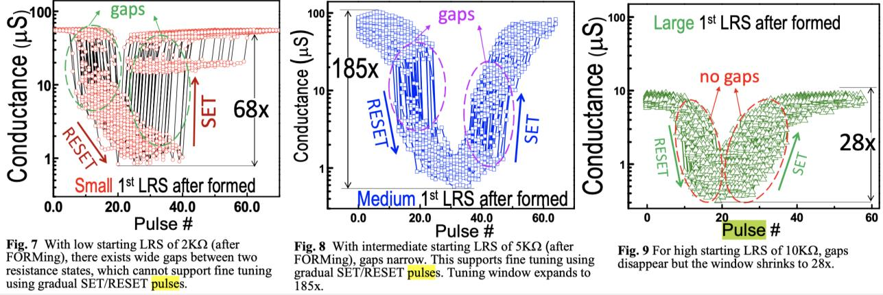
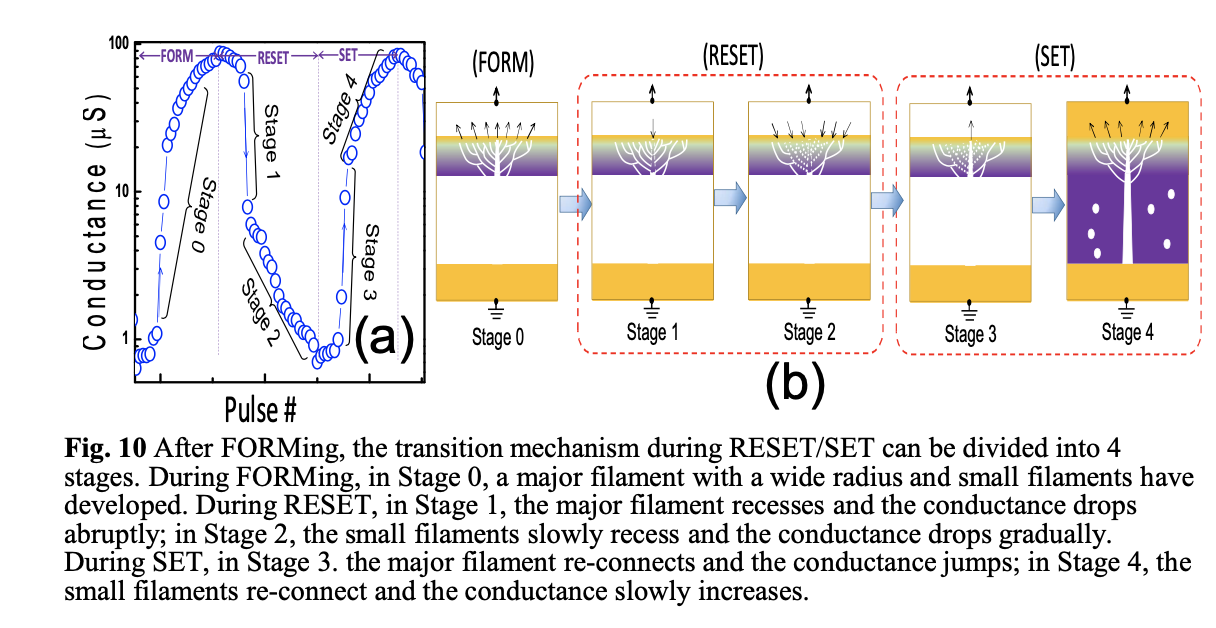
Fig. 10 provides a possible explanation for the results in Figs.7-9. We can divide the transition curve of conductance into 4 stages. During FORMing, in Stage 0, a major filament with a wide radius is created in HfO2. In addition, small filaments extend from the tip of the major filament to the top electrode. During RESET, in Stage 1, the major filament recesses resulting in abrupt drop in conductance. In Stage 2, the small filaments slowly recess resulting in gradual reduction of conductance. During SET, in Stage 3, the major filament reconnects and the conductance jumps. In Stage 4, the small filaments re-connect and the conductance slowly increases.
SETing/RESETing
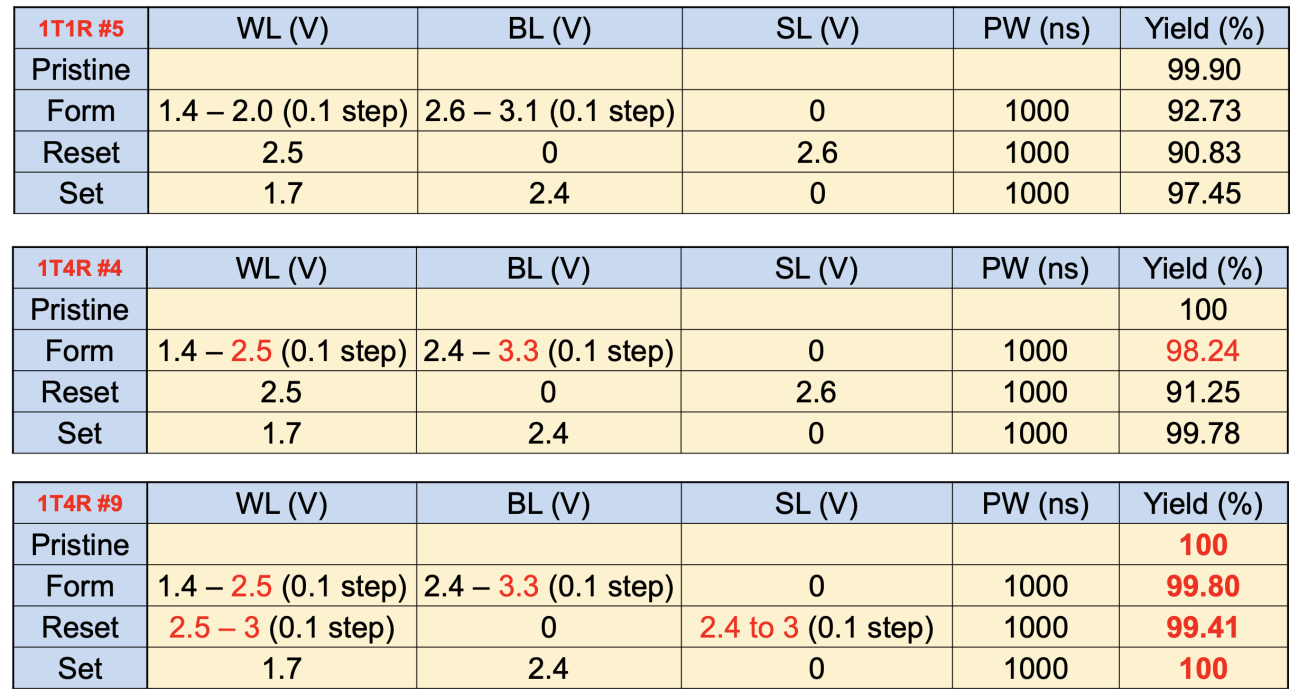
The standard SET/RESET pulses used with the SkyWater RRAM characteristics are summarized below for binary (e.g., 1-bit/cell) RRAM. Note that these are dependent on the initial forming conditions used (as discussed above). For completeness we give those conditions as well. Where a range is given, the procedure is as follows: first fix the BL voltage (for FORM/SET, SL voltage for RESET) and increase the WL pulse amplitude by the step size given until the cell is successfully formed/set/reset. If the cell is unsuccessful, then increase the BL voltage by the step size, and so forth.
The following tables were manually transcribed into this format the
original png is is provided so
that others may check the transcription.
1T1R #5 |
WL (V) |
BL (V) |
SL (V) |
PW (ns) |
Yield (%) |
|---|---|---|---|---|---|
Pristine |
99.90 |
||||
Form |
1.4 - 2.0 (0.1 step) |
2.6 - 3.1 (0.1 step) |
0 |
1000 |
92.73 |
Reset |
2.5 |
0 |
2.6 |
1000 |
90.83 |
Set |
1.7 |
2.4 |
0 |
1000 |
97.45 |
1T4R #4 |
WL (V) |
BL (V) |
SL (V) |
PW (ns) |
Yield (%) |
|---|---|---|---|---|---|
Pristine |
100.00 |
||||
Form |
1.4 - 2.5 (0.1 step) |
2.4 - 3.3 (0.1 step) |
0 |
1000 |
98.24 |
Reset |
2.5 |
0 |
2.6 |
1000 |
91.25 |
Set |
1.7 |
2.4 |
0 |
1000 |
99.78 |
1T4R #9 |
WL (V) |
BL (V) |
SL (V) |
PW (ns) |
Yield (%) |
|---|---|---|---|---|---|
Pristine |
100.00 |
||||
Form |
1.4 - 2.5 (0.1 step) |
2.4 - 3.3 (0.1 step) |
0 |
1000 |
99.80 |
Reset |
2.5 - 3.0 (0.1 step) |
0 |
2.4 - 3.0 (0.1 step) |
1000 |
99.41 |
Set |
1.7 |
2.4 |
0 |
1000 |
100.00 |
Alternative programming schemes can be used. For example, from our data on the 1T4R test #9 above, one could consider using a fixed reset pulse of WL=3V, SL=3V with a 1000ns pulse to ensure high RESET yields. Additionally, a lower voltage can be tried multiple times (e.g., a SET/READ and verify, or RESET/READ and verify) until the operation is successful. The pulse length is also a free variable, shorter (e.g., 100-200ns SET/RESET) pulses, with a verify scheme can also be used to reduce average write time.
Technology Specs: SkyWater 1T(n)R and Multiple Bits-Per-Cell
1T(n)R
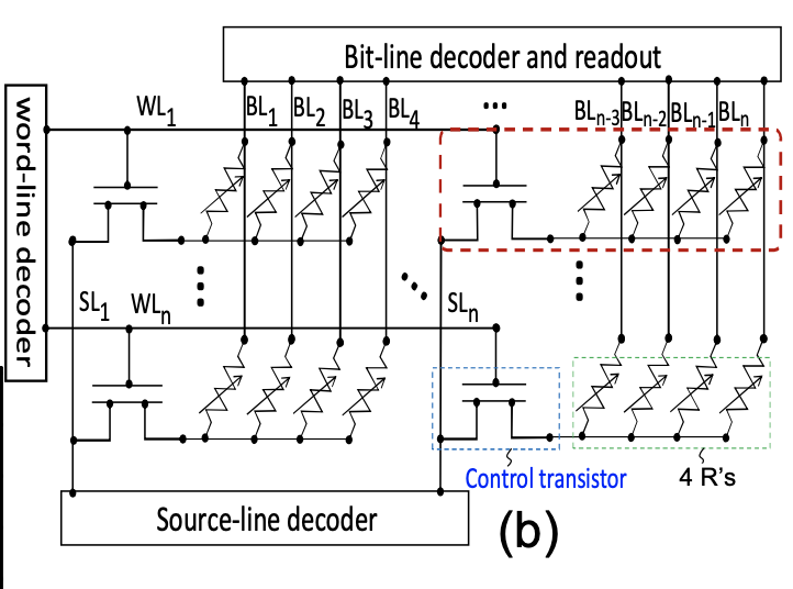
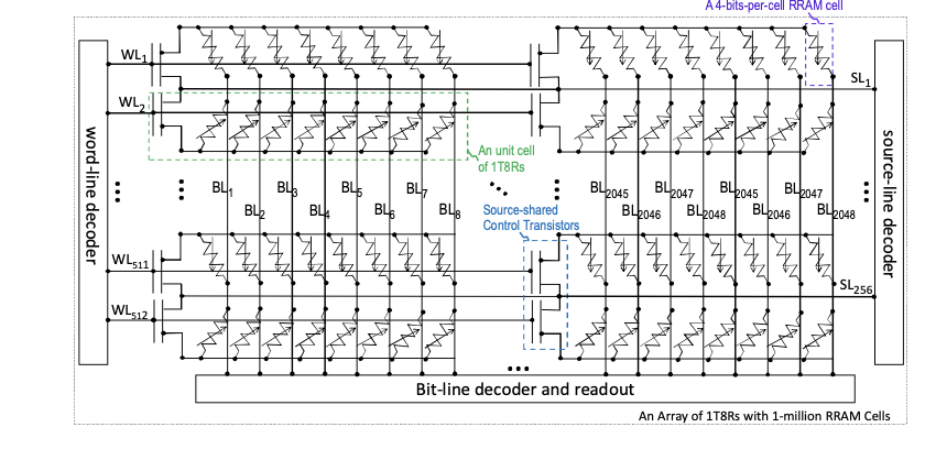
Multiple RRAM cells can be controlled with a single transistor. Such a layout increases density, especially when integrated monolithically (with multiple RRAM’s stacked above a single transistor). Below we give schematics of such 1T4R and 1T8R arrays.
FORMing 1T(n)R
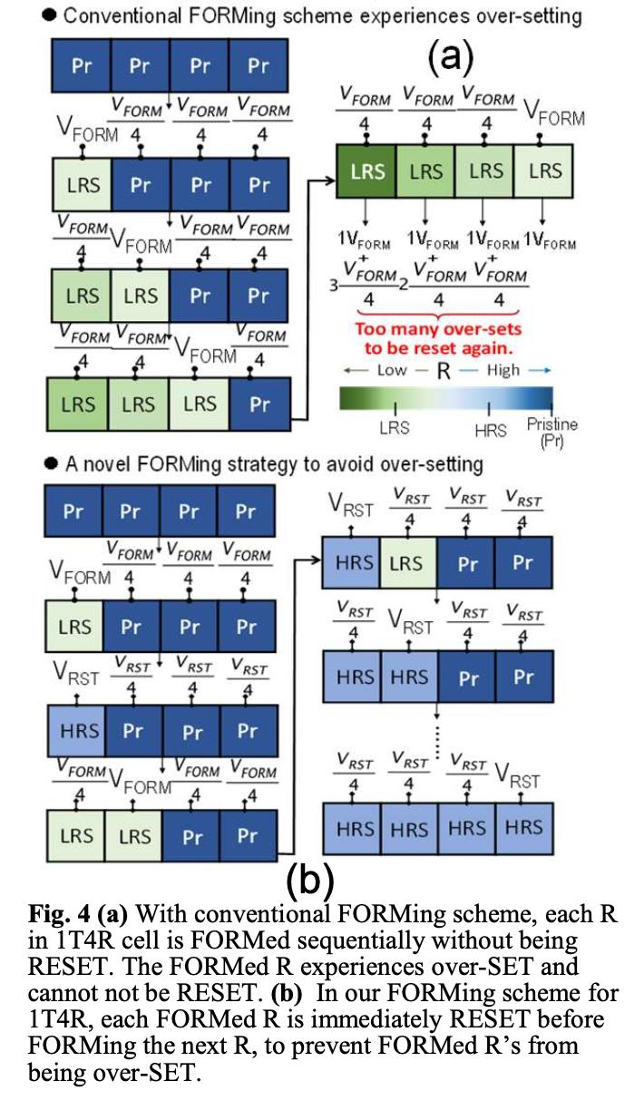
Such arrays require a different forming scheme. The operation of a 1T4R RRAM array is much more complex (vs. a 1T1R array) since interactions between multiple cells (in the same 1T4R structure) Fig. 4 presents our forming approach for 1T4R RRAM array. The conventional approach for 1T1R FORMs a cell (i.e., induces LRS in that cell) and then proceeds to the next cell. However, if this conventional scheme is directly applied to 1T4R (Fig. 4a), the FORMed cell, which is already in the low-resistance state (LRS), will experience additional SET (over-SET) as another cell inside the same 4R structure is being FORMed. After experiencing multiple over-SETs, the resistance of a FROMed cell may fall to an ultra-low value, and it may not be possible to RESET that cell anymore. The FORMing scheme in Fig. 4b overcomes this challenge by RESETting a cell (to the high-resistance state or HRS) immediately after it is FORMed. Therefore, when a cell is being FORMed, the adjacent FROMed but RESET cells (in the same 1T4R structure) are no longer over-SET. Occasionally, an adjacent RESET cell may be SET accidentally. It is necessary to check and RESET all cells in the 1T4R structure before the next cell is FORMed. Using this strategy, the FORMing yield is 99%. The forming voltages were given in the tables above.
SETing/RESETing 1T(n)R
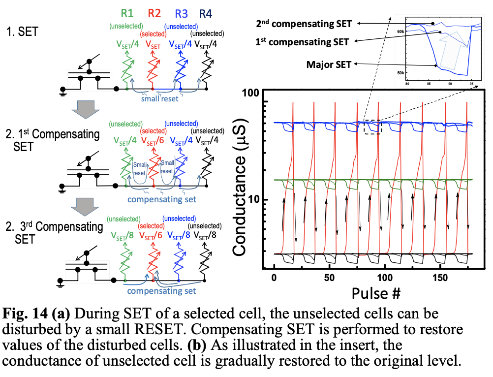
While the voltages of SET/RESET are given in the tables above, there are additional considerations in writing a 1TnR cell. Multiple bits-per-cell operation of 1T4R RRAM requires more precise control (vs. 1T1R) since disturbances between adjacent cells (in the same 1T4R structure) will be more serious. For example, Fig. 14 shows that when a cell in 1T4R is selected to be SET, the other 3 (unselected) cells can experience a small RESET, which can disturb the values stored in those (unselected) cells. Therefore, additional compensating SET operations are needed to restore the values in those (unselected) cells. By applying the compensating SETs, the disturbances in the unselected cells can be well alleviated, as shown in the insert of Fig. 14. The few low- voltage compensating SET pulses do not affect the other cells.
Multiple Bits-Per-Cell: 1T1R with 2 or 3 Bits-Per-Cell
Programming
Multiple bits-per-cell programming requires fine control over the cell resistance in order for the cells to end up in the desired range. There are two techniques that have been explored on the SkyWater RRAM, the first is demonstrated on a 1T1R structure and can achieve 2 or 3 bits-percell. Adjusting VWL allows for “coarse” tuning of the RRAM resistance (relatively large resistance change per pulse, but with less accuracy), while VBL and VSL allow for “fine” tuning (relatively small resistance change per pulse, but with more accuracy). Fig. 4 depicts the “tuning curves” at 6kOhm (representative resistance for illustration) in the SkyWater technology, which shows how the cell resistance (slope) is more sensitive to changes in VWL than to changes in VBL (for SET) and VSL (for RESET). A smaller slope signifies that the resistance can be tuned more slowly/accurately and indicates that voltage noise has a reduced impact on the change in resistance. We see that SET operations allow for finer tuning than RESET operations, since the SET operation results in an increasing voltage drop across the select transistor and a decreasing voltage drop across the RRAM cell.
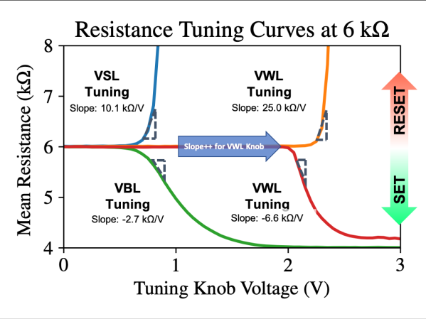
Fig. 5 Tuning curves showing the sensitivity of resistance change to different input knobs for a representative starting resistance of 6kΩ. Slopes are measured at 5.5kΩ for SET and 6.5kΩ for RESET. During VSL RESET tuning, VWL=3.5V; during VBL SET tuning, VWL=3V; for VWL RESET tuning, VSL=2.8V; for VWL SET tuning, VBL=2V. Data is averaged across 50 cells with 10 samples per cell. We also tested different starting resistances and step sizes (not plotted for clarity). For all parameters tested, the data showed that resistance change is more gradual when tuning with VBL/VSL rather than VWL.
References
- 1
E. R. Hsieh et al., “High-Density Multiple Bits-per-Cell 1T4R RRAM Array with Gradual SET/RESET and its Effectiveness for Deep Learning,” 2019 IEEE International Electron Devices Meeting (IEDM), San Francisco, CA, USA, 2019, pp. 35.6.1-35.6.4, doi: 10.1109/IEDM19573.2019.8993514.