Background
A typical Resistive RAM (RRAM) device consists of a metal-oxide switching layer (e.g., HfOx, TaOx, TiOx, AlOx by atomic layer deposition) sandwiched by top and bottom metal electrodes, forming a two-terminal metal-insulator-metal (MIM) structure. As a CMOS-compatible NVM device, RRAM can be directly fabricated in the back-end-of-line (BEOL) process without impacting the front-end-of-line (FEOL) portion of a silicon chip. [1] At SkyWater Technology Foundry, a HfO2-based RRAM layer is fabricated within the BEOL process at multiple points as described in the physical design rules.
General Operation
RRAM’s general operation is as follows: an applied electric field across the electrodes induces the creation and motion of oxygen vacancies within the insulator oxide, resulting in the formation of conductive filaments in the oxide. This changes the device resistance, which varies between high and low states. [2] There are thus three distinct modes of operation:
Forming, (also referred herein as FORM) during which an initial oxygen filament is created.
Writing, during which the conductivity of this filament is manipulated by the application of electric field.
Reading, during which the resistance or conductivity of the filament is sensed and converted into a digital value.
During forming, a high electric field is applied to form the filament. The fresh (un-formed) RRAM cell starts at an ultra-high resistance (ultra-low conductance state), through the creation of the initial filament via the formation of oxygen vacancies, a low resistance state (high conductance state) is reached. Writing can be further broken down into two distinct modes:
RESET – in which resistance is increased (conductance decreased) by applying a negative electric field across the device bringing it from a low resistance state (LRS) to a high resistance state (HRS)
SET – in which resistance is decreased (conductance increased) by applying a positive electric field across the device brining it from HRS to LRS. The voltages applied during SET/RESET are usually of lower magnitude than forming. Reading is usually performed with a low-applied voltage (e.g., 0.1-0.2V) using current sensing to determine the state of the RRAM device; often the HRS is used to store a logical ‘0’ and the LRS stores a logical ‘1’. RRAM setup usually follows this sequence: FORM -> RESET -> SET. Leaving cells all in a LRS ‘1’ state. Additional SET/RESET cycling can be performed to improve the switching reliability, and leave cells in a specified state.
Beyond a single RRAM cell, arrays require the use of a control transistor, creating a 1T-1R structure. This control device is used both to select the cell within the array but also controls the compliance current during the FORM, SET, and RESET operations. When thinking about an RRAM-based system, all three modes must be supported in order to enable system functionality: e.g., built-in forming must be enabled, otherwise the RRAM will be non-functional (e.g., SET and RESET operations have no impact unless the cell filament is first FORMed).
A general RRAM cell schematic, technology, and array architecture are shown in Fig. 1 and Fig. 2 shows the schematic of the three inputs to an RRAM cell, namely the bitline (BL), wordline (WL), and source line (SL). The voltages at these inputs can be used as “knobs” to program the cell resistance to a target range. The wordline voltage (VWL) controls the compliance current through the RRAM cell, while the bitline voltage (VBL) and source line voltage (VSL) control the potential across the cell. In order to perform a SET operation, VBL is increased while VSL is grounded. To perform a RESET operation, VSL is increased while VBL is grounded. For both SET and RESET, VWL must be above the threshold voltage of the control transistor to enable current flow through the cell.
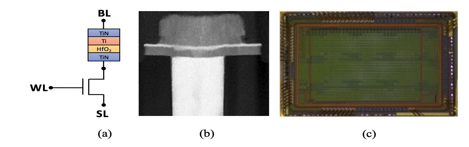
Fig. 1 (a) Cell schematic, (b) RRAM cell TEM, and (c) die photo of array.
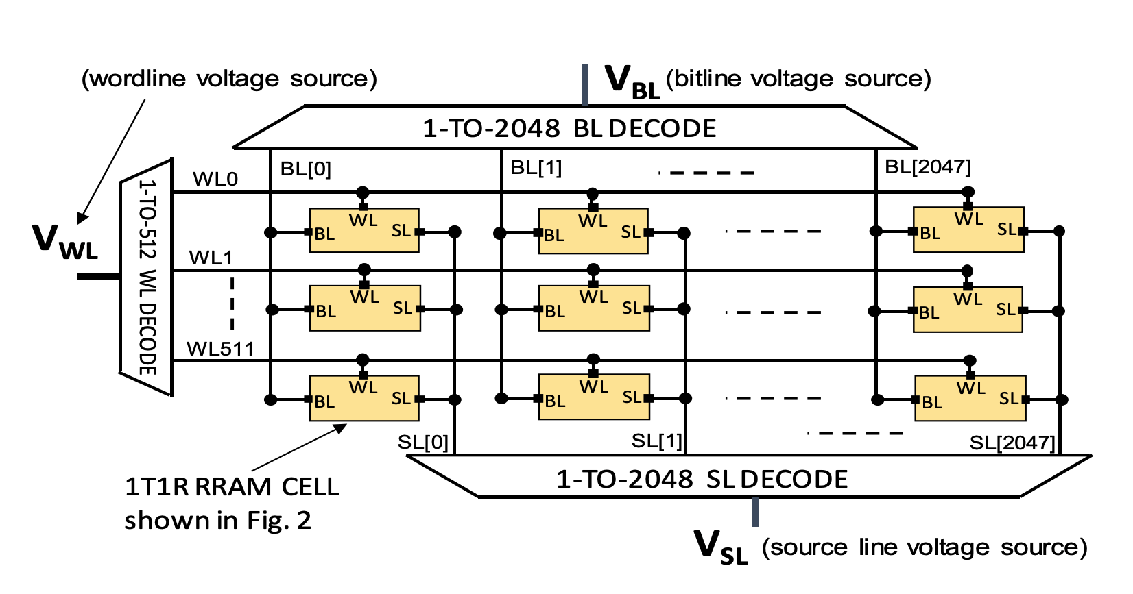
Fig. 2 1T1R RRAM array architecture
Beyond monolithic integration, the use of RRAM arrays offers many benefits at the system level:
RRAM inherently promises higher memory density compared to SRAM due to its 1T1R structure.
RRAM offers low read energy and latency, due the low voltage of reading and large resistance window between HRS and LRS.
RRAM is non-volatile, power is not required to maintain an RRAM’s resistance value; RRAM-based systems can thus be quickly turned on and off enabling fine-grained temporal power gating [4].
Additional structures beyond 1T1R (e.g., 1TnR), when monolithically integrated, provide RRAM even greater densities [3].
RRAM can support multiple bits-per-cell storage, effectively boosting storage density [3].
Multiple bits-per-cell storage in RRAM requires dividing up the resistance range into multiple levels (e.g., not just the single LRS and HRS of a binary 1-bit cell). These levels can be specified by a set of ranges and gaps, where cells are considered to be in one digital level if their resistance is within the corresponding range, and a cell is in error if left in the gap. This scheme is demonstrated in Fig. 3.
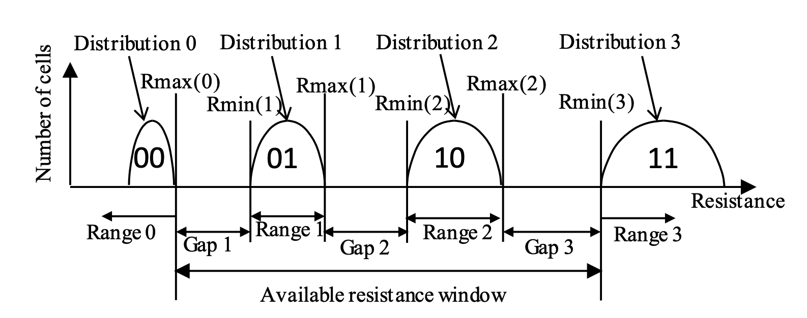
Fig. 3 Ranges and gaps in 2 bits-per-cell RRAM
RRAM cells, after forming, have an available resistance window between the lowest resistance states achievable and the highest resistance state achievable (e.g., the LRS and HRS used in binary storage). Determining how to optimally partition this window for the additional levels in 2-bit, 3-bit and beyond storage is currently under research. In later sections we will discuss one such technique and show the measured performance achievable with the SkyWater RRAM technology. Two additional ideas that are key to understanding RRAM’s capabilities are the following: retention, e.g., the ability for the RRAM’s resistance to stay constant throughout time (either with or without power) and endurance, the limited number of SET-(writing a ‘1’)–RESET-(writing a ‘0’) cycles a memory cell can undergo before permanent write failure (stuck at the ‘1’ or ‘0’ state). RRAM’s major benefits come with some additional challenges that must be considered in design, namely:
Compared to reads, RRAM has relatively higher write energies and latencies.
RRAM has limited endurance compared to volatile technologies like SRAM and DRAM
RRAM faces potential retention challenges at very high temperatures, especially if using multiple bits-per-cell storage (this will be In the following sections, we provide detailed data quantifying the RRAM technology provided at SkyWater.
This technology is still under development and the following procedures do not guarantee the results indicated. This document will be updated as necessary to provide the most current data on the process.
References
- 1
Rich D. et al. (2020) Heterogeneous 3D Nano-systems: The N3XT Approach?. In: Murmann B., Hoefflinger B. (eds) NANO-CHIPS 2030. The Frontiers Collection. Springer, Cham. https://doi-org.stanford.idm.oclc.org/10.1007/978-3-030-18338-7_9
- 2
Wong, HS., Salahuddin, S. Memory leads the way to better computing. Nature Nanotech 10, 191–194 (2015). https://doi-org.stanford.idm.oclc.org/10.1038/nnano.2015.29
- 3(1,2)
E. R. Hsieh et al., “High-Density Multiple Bits-per-Cell 1T4R RRAM Array with Gradual SET/RESET and its Effectiveness for Deep Learning,” 2019 IEEE International Electron Devices Meeting (IEDM), San Francisco, CA, USA, 2019, pp. 35.6.1-35.6.4, doi: 10.1109/IEDM19573.2019.8993514.
- 4
T. F. Wu, B. Q. Le, R. Radway, A. Bartolo, W. Hwang, S. Jeong, H. Li, P. Tandon, E. Vianello, P. Vivet, E. Nowak, M. K. Wooters, H.-S. P. Wong, M. M. Sabry Aly, E. Beigne, S. Mitra “14.3 A 43pJ/Cycle Non-Volatile Microcontroller with 4.7μs Shutdown/Wake-up Integrating 2.3-bit/Cell Resistive RAM and Resilience Techniques,” 2019 IEEE International Solid- State Circuits Conference - (ISSCC), San Francisco, CA, USA, 2019, pp. 226-228, DOI: 10.1109/ISSCC.2019.8662402
- 5
B. Q. Le, A. Grossi, E. Vianello, T. Wu, G. Lama, E. Beigne, H.-S. P. Wong, S. Mitra, “Resistive RAM with Multiple Bits per Cell: Array-Level Demonstration of 3 Bits per Cell,” IEEE Transactions on Electron Devices Journal, vol. 66, Issue 1, Jan. 2019. 10.1109/TED.2018.2879788